


 Crypto.
 Environ
 Passport
 Conference call
 send money
 Conditions générale de vente
 Confidentialité
 Sierra market
Technological Advancements In Backside Illumination And Deep Cooling Redefining High Performance Sensing
Technological advancements across modern sensor manufacturing and cryogenic packaging methodologies are reshaping application capabilities, as reflected in current Ccd Image Sensors Market Trends favoring back-thinned architectures, enhanced ultraviolet sensitivity, and intelligent readout electronics. Historically, front-illuminated charge-coupled devices encountered fundamental physical limitations due to the polycrystalline silicon gate electrodes deposited across the front surface of the sensor substrate. These opaque gate structures absorb a notable percentage of incoming photons, particularly in the ultraviolet and blue spectral wavelengths, curbing overall quantum efficiency. To overcome this limitation, specialized wafer foundries apply precision chemical-mechanical planarization and selective etching techniques to thin the rear silicon substrate down to ten to fifteen micrometers. By illuminating the sensor from the back, incoming photons strike the active silicon depletion layer directly without obstruction, elevating quantum efficiency values beyond ninety percent in targeted visible and near-infrared spectrum ranges.
Another prominent trend within specialized scientific imaging is the integration of advanced anti-reflective surface coatings and specialized luminescent phosphors to expand spectral capture across extreme wavelengths. Back-illuminated sensors treated with specialized broadband anti-reflective thin films prevent photon bounce-back, optimizing detection across soft x-ray, vacuum ultraviolet (VUV), and extreme ultraviolet (EUV) spectral bands. These specialized variants find widespread adoption in next-generation semiconductor photolithography inspection stations, where manufacturers verify the structural integrity of extreme ultraviolet pellicles and photo-masks. Furthermore, in plasma physics experiments and synchrotron radiation research, charge-coupled arrays equipped with direct x-ray detection capabilities provide structural insight into atomic lattices without requiring external conversion scintillators. This direct-detection capability avoids intermediate photon conversion steps, maximizing spatial resolution and energy-dispersive measurement accuracy.
Simultaneously, thermal management and vacuum enclosure technologies have advanced considerably, enabling deep thermoelectric cooling in compact, field-deployable camera form factors. To achieve maximum signal clarity during long-exposure scientific imaging, thermal generation of electron-hole pairs—known as dark current—must be minimized. Modern scientific cameras incorporate hermetically sealed, vacuum-insulated sensor chambers backfilled with noble gas mixtures or maintained under permanent ultra-high vacuum conditions. Multi-stage Peltier thermoelectric coolers coupled with integrated liquid heat exchangers pull sensor operating temperatures down to minus one hundred degrees Celsius without inducing condensation or structural stress. At these cryogenic temperatures, dark current levels drop to fractions of an electron per pixel per hour, allowing astrophysicists and forensic investigators to conduct integration times spanning hours to register faint spatial signals that would otherwise remain undetectable.
Furthermore, digital readout controllers and multi-channel output architectures are evolving to reduce readout times while maintaining pristine signal integrity. Charge-coupled devices are traditionally constrained by serial readout topologies that produce slower frame rates when compared with massively parallel CMOS column-readout designs. To mitigate this operational bottleneck, modern scientific sensors feature multi-port architectures, splitting the image array into four or more independent quadrants, each served by a dedicated low-noise output amplifier and analog-to-digital converter (ADC). By reading pixel data concurrently across multiple channels, modern cameras achieve high frame rates suitable for real-time laser beam profiling, adaptive optics wave-front sensing, and in vivo bio-imaging. These engineering refinements ensure that charge-coupled sensors remain at the forefront of cutting-edge scientific discovery, delivering unmatched sensitivity and measurement accuracy across demanding research disciplines.
Top Trending Reports :
Computer Vision Ai Artificial Intelligence Camera Market
Computer Vision Technologies Market
Connected Solutions For The Oil And Gas Market
Consumer Active Optical Cable Market
Consumer Electronic Biometric Market
Bub
Do?

Catégories
Lire la suite
You run a small retail shop on a busy street in Abu Dhabi. You want your shelves stocked with new items every single week. You want your cash flow to stay strong and steady. But tracking every dirham of income can feel very hard. Many business owners mix personal cash with business funds. You feel stuck when tax season arrives with messy receipts. You need a smart way to keep your ledger...

Visionaries reshaping studio hierarchies emerge from diverse career paths Beyond conventional resumes, these innovators redefine leadership potential Dealmaking prowess distinguishes rising power brokers Armyan Bernstein crafts indie success stories while resisting corporate capture Ari Emmanuel executes with relentless efficiency, transforming agency influence Franchise architects...

Hero Development and Strategy Achieving victory in PvE challenges like Crazy Joe and Bear Hunt requires strategic hero deployment and development. Similarly, excelling in PvP battles such as SVS and Brothers in Arms hinges on selecting the right heroes and optimizing their abilities. Your heroes play a pivotal role in shaping your overall performance, making their effective management...
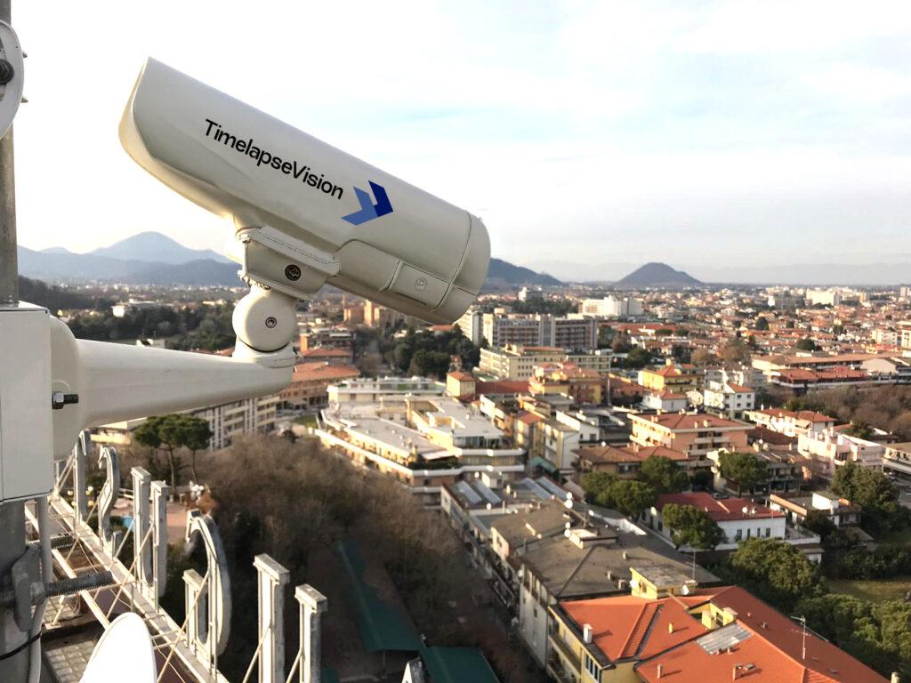
Nel settore delle costruzioni, il controllo efficace del cantiere è essenziale per garantire il successo di un progetto. Oggi le imprese edili devono affrontare sfide sempre più complesse legate alla gestione delle attività operative, alla sicurezza dei lavoratori e al rispetto delle tempistiche. Per questo motivo il monitoraggio remoto dei cantieri...
I grew up on the "real" Monopoly too, the kind that eats your whole evening and ends with someone storming off over rent. So when Monopoly Go showed up on my phone, I rolled my eyes. Then I tried it on a break, got sucked in, and suddenly I was thinking about dice rolls while the kettle boiled. If you're the type who keeps an eye on limited-time stuff like Racers Event slots buy offers, the...